WL1610 is a type of low cost, high integration intensity, high
transmit power and 2.4 GHZ wireless transceiver chip, where are integrated with
transmitter,receiver,frequency synthesizer GFSK and modulator-demodulator.
WL1610 has advantages of high sensitivity, low power consumption and strong
antijamming capacity. It’s suitable for wireless remote control, wireless
communication,industrial control and other fields.
FIFO
register to send and receive on the chip can communicate and conduct data
storage with MCU, and can transmit in air with the max data rate of 1Mbps. It’s
built in with CRC, FEC, Auto-ACK and retransmission system, which can hugely
simplify system design and optimize performance. At the same time, it has
simple peripheral circuit, and only has to be matched with MCU and a few
peripheral passive devices. To improve the using life of battery, chip will
reduce its power dissipation in each link. The lowest working pressure of chip
can be 1.9 V. The lowest sleep mode electricity is less than 1uA. Digital
baseband support 4-line SPI and 2-line I2C connector. PKT_FLAG digital
connector can be as the interrupted input of MCU.
2、Key Features
l 2.4GHz ISM-Band Low-Power, GFSK
RF transceiver
l Max air data rate 1Mbps,min
air data rate 32Kbps
l DSSS MODEM
l Embedded 8-bit framer with 64-byte buffer offloads MCU for other
tasks
l Simple
microprocessor interface – SPI, I2C
l Great
C/I provides excellent WIFI coexisting performance
l Programmable
data whitening and auto_ack
l Supports
Forward Error Correction (FEC), Increases the reliability of communication
l Supports
8/16-bit CRC
l Supports
AGC
l Power management for minimizing current consumption (<1uA sleep
current)
l Tolerant crystal with variation up to 50PPM
l FCC/ETSI compliance
l 110℃ operating temperature, applies to LED light ( crystal’s PPM
within ±50ppm
)
l Close-up
mode for environments with specific security requirements
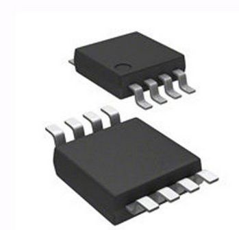
l Supports QFN20, SOP16 packages
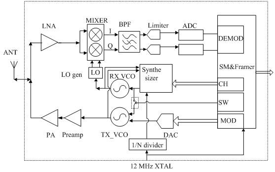
3、Block Diagram
Figure 1 WL1610 Block Diagram
4、Electrical Characteristics
Chart 1electrical characteristics(TA=25°C, VDD=3.3V if
nothing else stated.)
Parameters
Description
Specification
Units
Notes
MIN
TYP
MAX
TOP
Operating Temperature
-40
85
℃
1610’s maximum operating temperature: 110 ℃
VDD
Power supply range
1.9
3.6
V
F_xtal
Crystal frequency
12
MHz
50PPM tolerance
IDD_TX
TX Current
95
mA
POUT = 17dBm
IDD_RX
RX Current
21
mA
IDD_IDLE
IDLE Current
1
mA
IDD_SLP
Sleep Current
1
uA
3.0v at Room temperature
FCLK
Output clock
12
MHz
Tr_spi
SPI_CLK rise, fall time
25
ns
Requirement for error-free register reading,writing.
F_SPI
SPI_CLK frequency range
0
12
MHz
F_OP
Operating Frequency Range
2400
2482
MHz
VSWR
Antenna port mismatch
(Z0=50W)
<2:1
VSWR
RXS
Receiver sensitivity
-103
-88
-83
dBm
BER <= 0.1%
RXM
Maximum useable signal
-10
dBm
BER <= 0.1%
IIP3
Input 3rd order intercept point
-15
-12
dBm
BER <= 0.1%
R_data
Data/Symbol Rate
32K
1M
Bit/s
CI_co-channel
Carrier/Interference at
co-channel
9
dB
CI_1MHz
Carrier/Interference at
1MHz offset
-1
dB
-60 dBm desired signal.
CI_2MHz
Carrier/Interference at
2MHz offset
-27
dB
-60 dBm desired signal.
CI_3MHz
Carrier/Interference at
3MHz offset
-35
dB
-60 dBm desired signal.
CI_Image
Carrier/Interference at
image frequency
-20
dB
-67 dBm desired signal.
CI_3MHzUp
Carrier/Interference at
>3MHz offset
-33
dB
-60 dBm desired signal.
OBB_1
Out-of-Band Blocking
-10
dBm
30 MHz to 2000 MHz
OBB_2
-27
dBm
2000 MHz to 2400 MHz
OBB_3
-10
dBm
3000 MHz to 12.75 GHz
Pout_max
Max RF Output Power
17
dBm
Power Level MAX
Pout
Min RF Output Power
0
dBm
Power Level MIN
DF1avg
Peak FM Deviation
00001111 pattern
250
kHz
Modulation Characteristics
TX EYE diagram
DF2max
Peak FM Deviation
01010101 pattern
220
kHz
Modulation Characteristics
TX EYE diagram
DF2max /DF1avg
TX EYE opening
80
%
1010 data sequencereferenced to 00001111 data
sequence
IBS_1
In-Band Spurious Emission
(+/- 550kHz)
-20
dBm
Random data
IBS_2
In-Band Spurious Emission
2MHz offset
-40
dBm
Random data
IBS_3
In-Band Spurious Emission
3MHz offset
-60
dBm
Random data
OBS_1
Out-of-Band Spurious Emission
-60
dBm
30 MHz ~ 1 GHz
OBS_2
-45
dBm
1 GHz ~ 12.75 GHz
OBS_3
-60
dBm
1.8 GHz ~ 1.9 GHz
OBS_4
-65
dBm
5.15GHz ~ 5.3 GHz
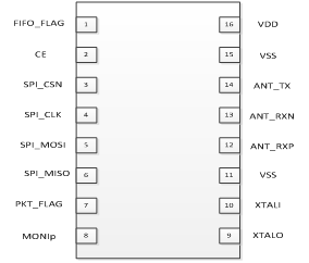
5、Pin Description
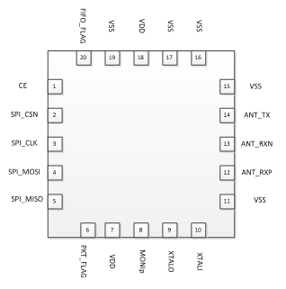
Figure 2
WL1610 pin assignments (top view) for the QFN20 package


 High TX power 2.4GHz RF Transceiver
 沪公网安备31011702002162号